 |
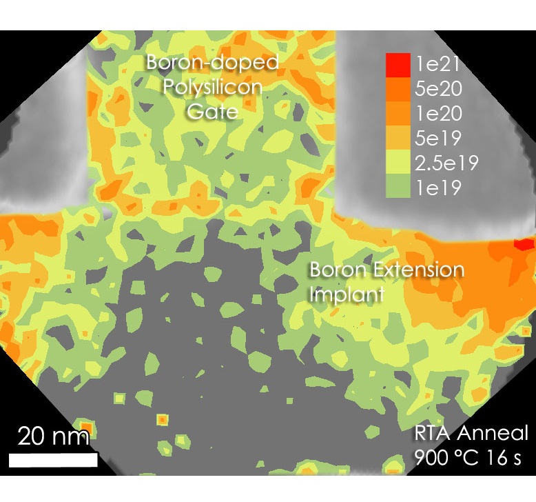
2D doping profile of ion-implanted B following rapid thermal annealling from an extension region of a CMOS FET device. Data was acquired using Local Electron Atom Probe (LEAP). |
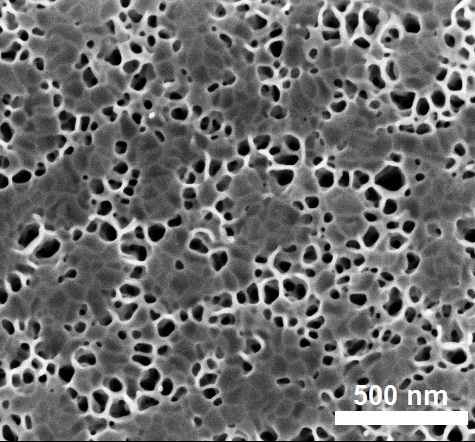 |
HRSEM plan-view image of 1E17 Ge implant into (001) Ge showing the resulting porous structure. |
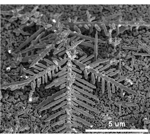 |
Ag dendrites formed from the reduction of silver ions in a 0.04M AgNO3/5M HF solution on a (001) silicon substrate. |
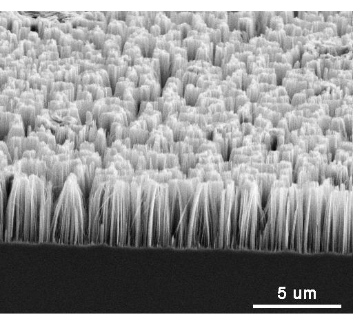 |
Si nanowire array formed from solution-based processing at room temperature and pressure. (001) Si wafer was submersed in 0.04M AgNO3/5M HF solution during which Ag is reduced and Si is selectively oxidized and etched to form SiNW array. Ag dendrites were stripped using HNO3. |
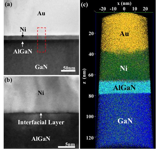 |
(a & b) TEM image of the gate region of an AlGaN/GaN HEMT structure (c) Reconstructed 3D atom probe (AP) data collected near gate metal stack/semiconducting epi-layer interface displaying the distinct Au, Ni, AlGaN, and GaN layers. The boxed area in part a indicates the approximate area analyzed by AP as shown in b. |
 |
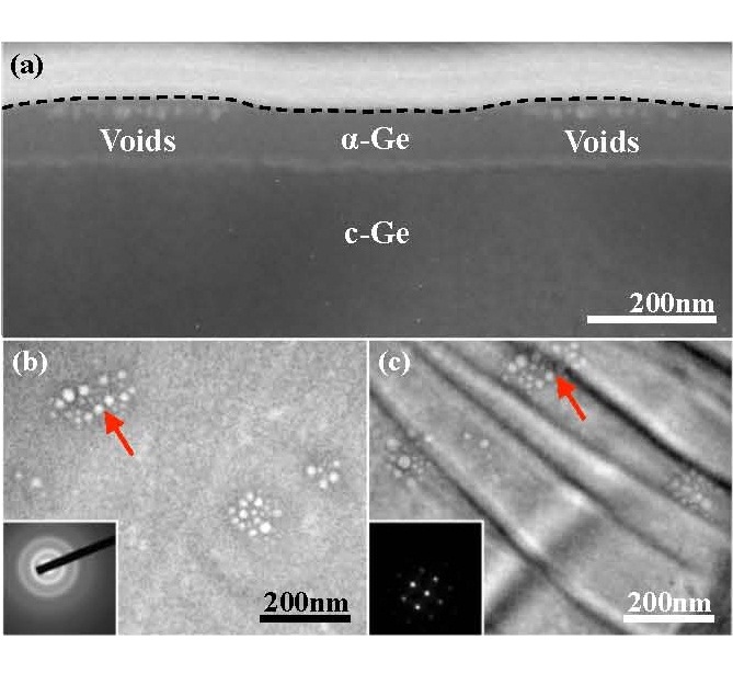
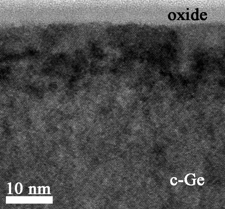
Cross-sectional TEM of a 1E17 Ge implant into deposited Ge on an Si substrate. |
 |
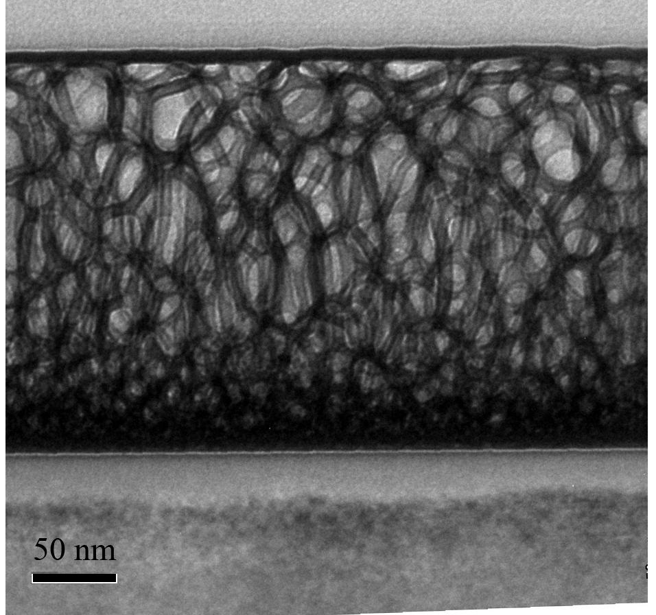
Cross-sectional and plan-vew TEM images of void clusters created by 90 keV 2E15 Ge implants into (001) Ge. |
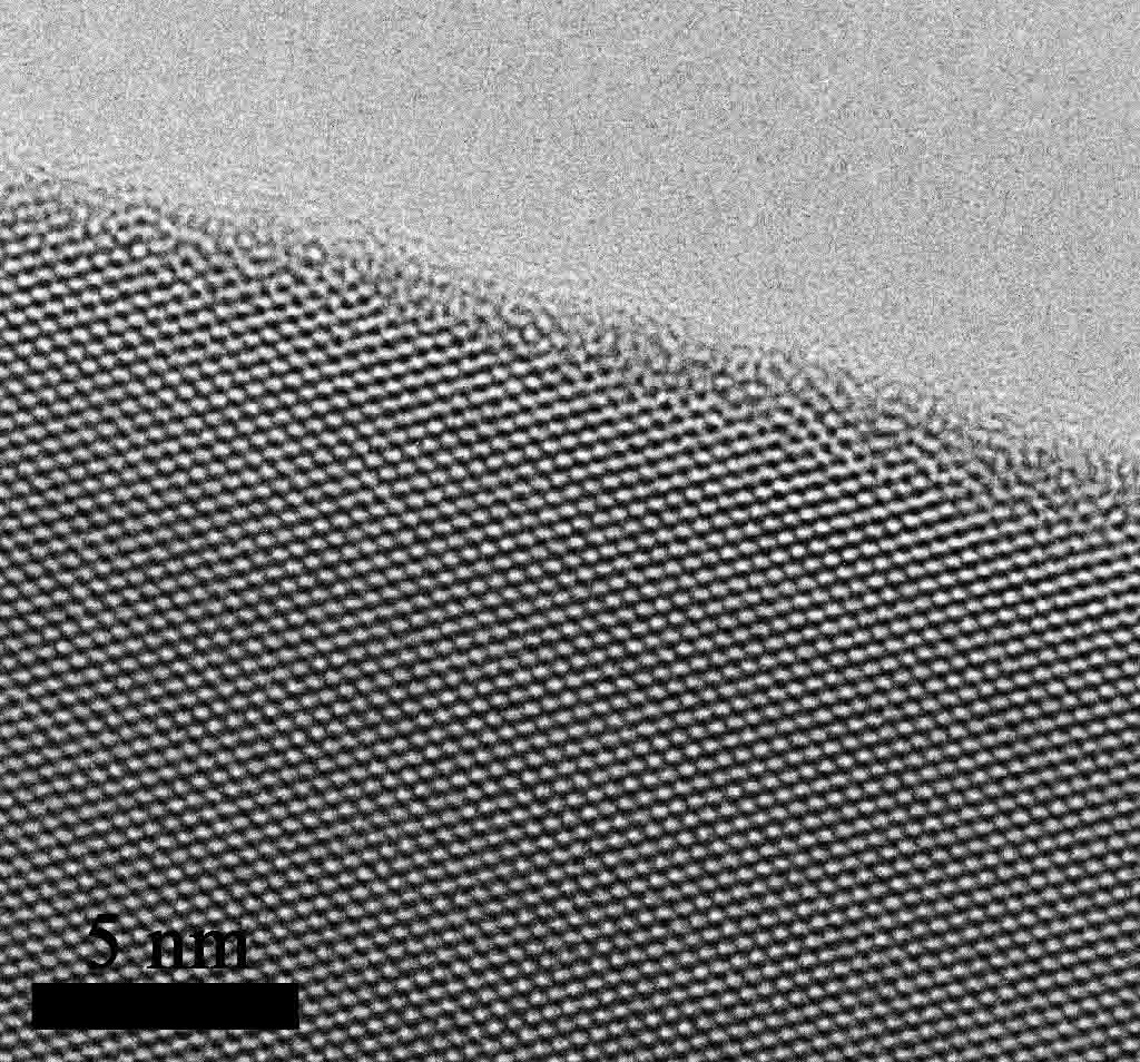 |
High-resolution transmission electron microscopy image of a Ge nanowire displaying the atomic resolution capabilities of the instrument. |
 |
HRTEM image of the as-implanted damage created by a 2keV 5E15 B/cm^2 implant into (001) Ge. |
